


Adp200er Schematic Exclusive !new! -
Based on circuit analyses from Haseeb Electronics and other repair experts, the board is divided into several main sections:
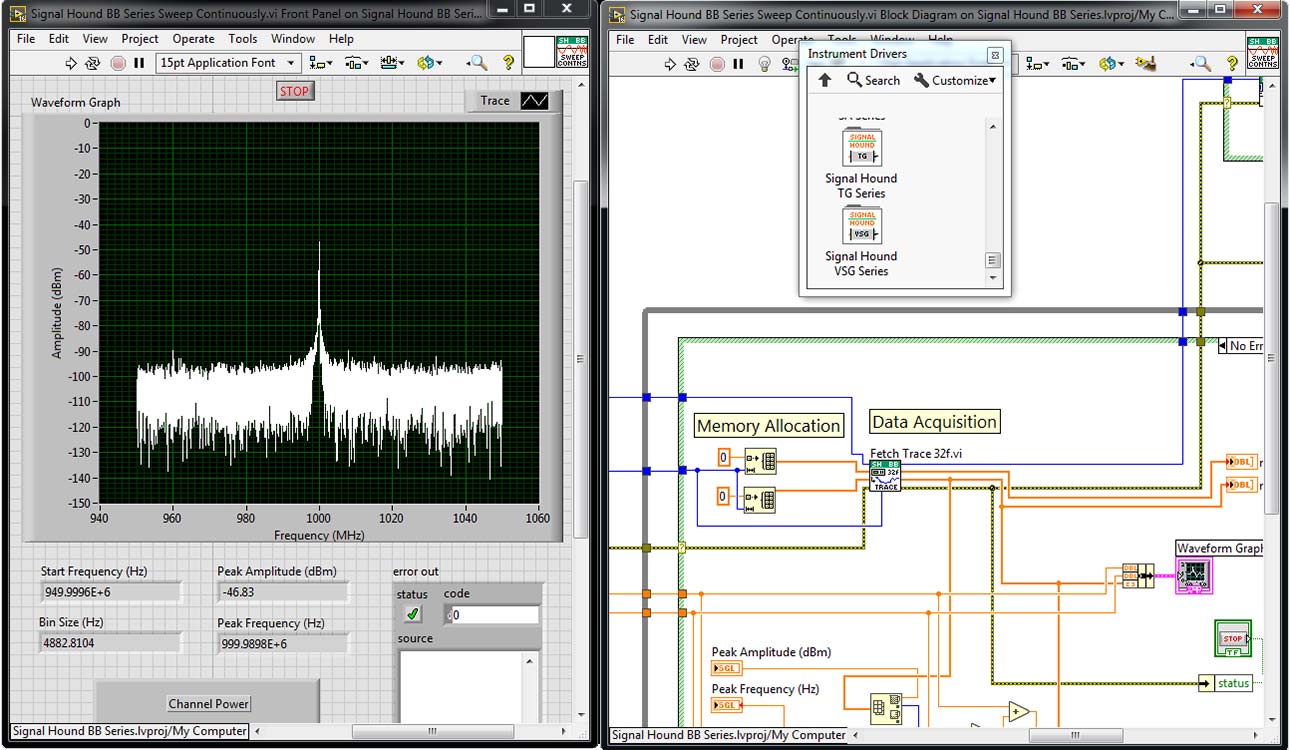
The ADP-200ER is a switched-mode power supply (SMPS) with several critical stages described in technical teardowns:
Start your search in the OEM repair archives (Lenovo, Delta, Foxconn). Verify the pinout details and the PMBus map. Avoid generic PDF scrapers. With the exclusive schematic in hand, you transform the ADP200ER from a mysterious black box into a predictable, fixable, and masterable piece of silicon. adp200er schematic exclusive
: While full factory diagrams are rare, detailed component lists and partial schematics are often archived on Scribd's PS4 PSU Guide .
. While "exclusive" official schematics from Sony are generally not publicly available, community-sourced guides and functional analyses provide detailed circuit descriptions for repair. The is a push-pull SMPS (Switched-Mode Power Supply) . AC Input: 100-240V~ 2.5A, 50/60Hz. DC Output: +4.8V (standby) at 1.5A and +12V (main) at 16A. Based on circuit analyses from Haseeb Electronics and
When diagnosing a dead or malfunctioning ADP-200ER board without a visual diagram, use this sequential testing protocol:
To check for short circuits on a repaired ADP-200ER board without damaging new components, use a series lightbulb circuit tester. PlayStation 4 ADP-200ER PSU repair - Badcaps With the exclusive schematic in hand, you transform
An exclusive schematic analysis divides the ADP-200ER into four primary functional blocks: 1. AC Input and EMI Filtering Stage
: This switching action boosts the variable voltage up to a stable, high-voltage 410V DC bus stored inside the primary bulk smoothing electrolytic capacitor. Stage 3: The Standby Flyback Loop